Infineon makes working power chips on 300-millimetre silicon carbide wafers
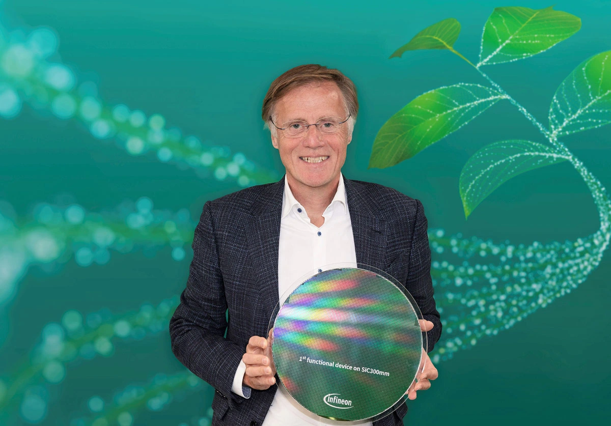
Jochen Hanebeck, Infineon CEO, with the 300-millimetre SiC wafer. Photo: Infineon, via Semiconductor Today.Pictured: Jochen Hanebeck (CEO, Infineon Technologies).Infineon has made working power-semiconductor devices on 300-millimetre silicon carbide wafers at its factory in Villach, Austria. The company announced the manufacturing demonstration on November 9, 2026. It used existing silicon-manufacturing equipment and describes the result as a first in a full-scale semiconductor factory environment.
A wafer is the round slice of semiconductor material on which many chips are made together. Silicon carbide, or SiC, is used in power electronics that convert and control electricity. It can operate efficiently at high voltages and temperatures, with uses including electric-vehicle power systems, industrial equipment, renewable energy and data-centre power supplies.
The larger wafer is the manufacturing change. Infineon states that a 300-millimetre wafer can provide 2.3 times as many chips as a 200-millimetre wafer. That is not a disclosed production yield or a measured reduction in the cost of finished chips: usable output also depends on defects, processing and qualification.
Infineon also reports that it has demonstrated the feasibility of its Cold Split process on 300-millimetre SiC material in Dresden. This process separates thin wafers from a larger SiC crystal with less material lost than conventional wire cutting. It is a separate manufacturing step from making devices on the wafer.
The announcement is a feasibility milestone, not the start of high-volume 300-millimetre SiC production. Infineon has not supplied a volume-production timetable, device specifications, electrical test results or production-yield figures in this release. It plans the technology and production ramp with customers and partners while continuing its 200-millimetre SiC roadmap.
A processed wafer is scheduled to be displayed at the electronica trade show in Munich, November 10-13. The reported first and the 2.3-times chip comparison remain company claims; the release does not establish lower finished-device costs or broad customer qualification.
DTT summary based on Infineon's report. The full article is on the publisher's site.
Additional reporting
Functional power devices processed on 300-millimetre SiC wafers at Villach.
Cold Split feasibility on 300-millimetre SiC material at Dresden.
No volume-production date or production-yield figures announced.