JNCASR chip guides high-speed data signals past obstacles
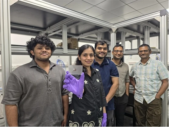
Research team at MetoLab, JNCASR, with the fabricated silicon chip. Photo: DST / PIB.Researchers at JNCASR in Bengaluru have built a silicon chip that helps data-carrying waves get past obstacles without losing much of their strength. In a lab test, one version carried 100 billion bits of data per second. The work could help researchers build small circuits for future 6G systems, but it is not a working 6G network.
Think of a signal travelling along a narrow road. Bends, junctions and obstacles can send some of it in the wrong direction, weakening what reaches the other end. The team made a pattern of tiny triangular holes in silicon to guide the signal along a chosen path. The waves used here are called terahertz waves: they sit between microwaves and infrared light.
The researchers then changed the hole sizes along a short stretch to create an obstacle. The signal could still pass with little extra loss. One obstacle added about 1-2% loss; two in a row added about 2-3%. The pattern worked within tested limits, not against every possible obstacle.
They tested three layouts. A path with two obstacles carried 48 billion bits per second. A winding path with four sharp bends carried 60 billion. A layout that split the signal into two branches reached 100 billion. These were different devices and tests, so the fastest number should not be read as the result for every layout.
Dr Abhishek Kumar led the work at JNCASR's Meta Optics Laboratory, or MetoLab. Samina Mulla and Sangram Kumar Sadhu were joint first authors. The study appeared in Advanced Materials, with collaborators in India, Singapore and France.
The useful idea is simple: change the pattern of holes to help control where a high-speed signal goes on a chip. Next, the team wants to change the paths using electricity, heat or mechanical movement. That could let a future device redirect a signal when needed. This remains laboratory research, not a product ready for phones or telecom networks.
DTT summary based on PIB / Department of Science & Technology's report. The full article is on the publisher's site.
Additional reporting
100 billion bits per second, on the layout that split the signal into two branches.
48 billion bits per second through two obstacles; 60 billion around four sharp bends.
Terahertz waves, between microwaves and infrared light. The measurements covered 310-360 GHz.
About 1-2% for one obstacle; 2-3% for two in a row, within the tested design limits.
A lab demonstration that could help future 6G circuits, not a commercial 6G network.