India opens Semicon 2.0 applications for chipmaking equipment, fabs and packaging
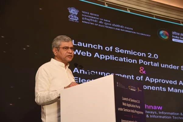
Ashwini Vaishnaw speaking at the Semicon 2.0 portal launch. Image: Press Information Bureau, November 6, 2026.India opened applications on November 6 for three parts of Semicon 2.0: machines and materials, chip factories, and chip assembly, testing and packaging. The Ministry of Electronics and Information Technology announced the portal launch alongside 12 approvals under a separate Electronics Components Manufacturing Scheme, or ECMS. These are application and project-approval milestones, not evidence that all the planned factories are operating.
The engineering focus is the machinery, chemicals, gases and materials used to make chips, alongside new fabrication plants and the facilities that assemble and test finished chips. A fab is a factory that builds circuits on semiconductor wafers. Assembly and packaging connect and protect the chips so they can be used in devices. Testing checks whether they work as intended.
Semicon 2.0 has an approved fiscal outlay of ₹1,27,500 crore, according to the ministry. Its six areas are chip design, machines and materials, more fabs, assembly and testing, research and development, and talent. The new portal initially accepts applications for machines/materials, fabs and assembly/testing. The announcement does not say applications are open across all six areas.
The 12 ECMS approvals carry projected investment of ₹7,503 crore and expected direct employment of 7,127. They cover items including multilayer printed-circuit boards, relays, heat sinks, specialist ceramics, battery materials and factory equipment. A printed-circuit board connects electronic components; a heat sink carries heat away from them. These projections are not money already spent, new grants awarded to each applicant or jobs already created.
The ministry named projects from NeST ICELR, TDConnex, Modern Automotives, Voltix Semicon, Indo Asia Copper, TACC, Vidyuta Materials, Enerfolie, Surface Modification Technologies, Rockwell Automation India and Wipro Pari Robotics. The list contains 12 approvals, including two different TDConnex activities, rather than 12 distinct companies. ECMS and Semicon 2.0 are separate programmes and their totals should not be added as one new chip-funding round.
Ashwini Vaishnaw also set a target of attracting at least three large equipment manufacturers and five chemicals and gases companies. That is an ambition, not a list of confirmed new factories. Separately, the ministry said five of the 12 projects approved under the earlier Semicon 1.0 programme had started commercial production by October 2026. That earlier operating count does not describe the new 12 ECMS approvals.
DTT summary based on Press Information Bureau's report. The full article is on the publisher's site.
Additional reporting
Applications opened November 6 for machines/materials, fabs and assembly/testing/packaging, not all six pillars.
₹1,27,500 crore approved fiscal outlay for Semicon 2.0; not a new company funding round.
12 approvals with ₹7,503 crore projected investment and 7,127 expected direct jobs. Projections are not money already deployed or jobs created.
Attract at least three equipment manufacturers and five chemicals/gases companies. Not confirmed new operating factories.